Hardware description
Table of contents
- Tour around the board
- Connectors
- ESP32 module
- Power supply
- Peripherals
- Buttons and LEDs
- USB
- CAN bus (NMEA 2000)
- I2C
- 1-Wire
- Optocoupler input and output
- GPIO header
- Proto board area
- Pinouts of peripherals
Tour around the board
Note: The pictures below show a Revision 1 board. Rev. 2 boards are functionally identical but have different power and CAN connectors and minor component changes.
The different functional blocks of SH-ESP32 are shown below.
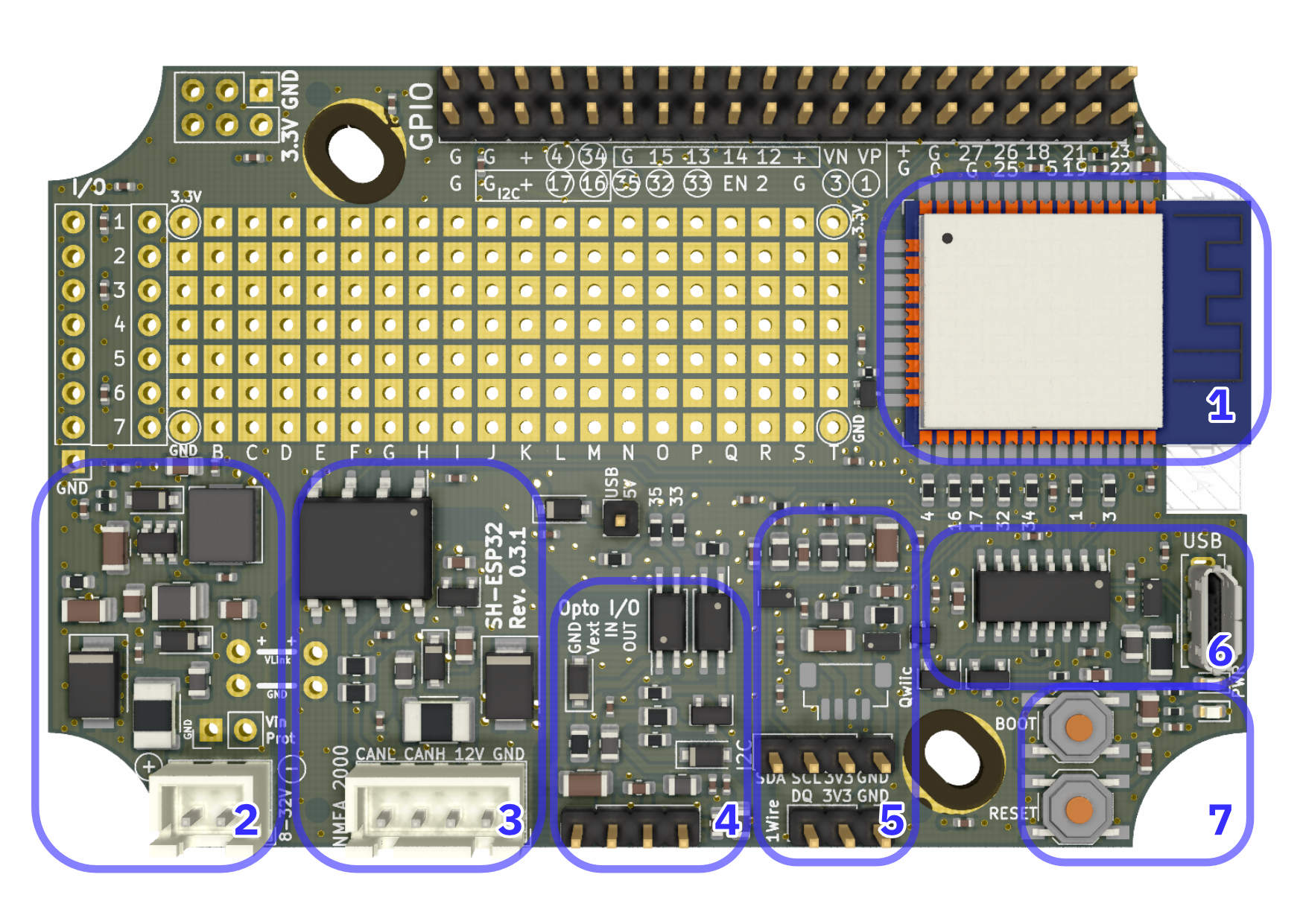 Functional blocks of SH-ESP32.
The ESP32-WROOM-32 module: The ESP32 microcontroller module is the heart of the device. It contains the two-core microcontroller with integrated RAM, a flash chip, and a WiFi/Bluetooth antenna (or, in the case of SH-ESP32-ufl, a U.FL connector for the antenna).
Power supply: SH-ESP32 has an integrated switching mode power supply that converts input voltages between 8V and 32V to the 3.3V voltage used on the board. The power supply also includes a self-resetting 500 mA polyfuse, reverse polarity protection, and surge protection.
CAN bus transceiver: SH-ESP32 includes an isolated CAN transceiver that conforms to the NMEA 2000 specification. The CAN bus circuitry also includes protection similar to the main power supply and a 5V linear regulator to power the transceiver independently from the NMEA 2000 bus.
Optocoupler input and output: Optocoupler I/O can be used to connect the SH-ESP32 safely to noisy external inputs or outputs such as the alternator signal or relays.
I2C and 1-Wire I/O: SH-ESP32 supports 1-Wire and I2C on separate 2.54 mm headers. Additionally, there is an unpopulated footprint for a Qwiic compatible JST SH connector. Both interfaces are ESD protected and have noise filtering.
USB interface: SH-ESP32 has a USB 2.0 compatible Micro B connector and interface. When connected to a host computer, the board is visible as a USB serial device. The USB interface can be used for powering the board, flashing the ESP32 module, and for communicating with the device using a serial protocol.
User interface: There are two buttons and two leds integrated on the board. The reset button resets the board. The boot button can be used to force the ESP32 into a flashing mode, and otherwise is usable as a generic button input on GPIO0. The red LED is hard-wired to the 3.3V power, indicating that the device is powered, while the blue LED is connected to GPIO2 and can be controlled by the program.
Connectors
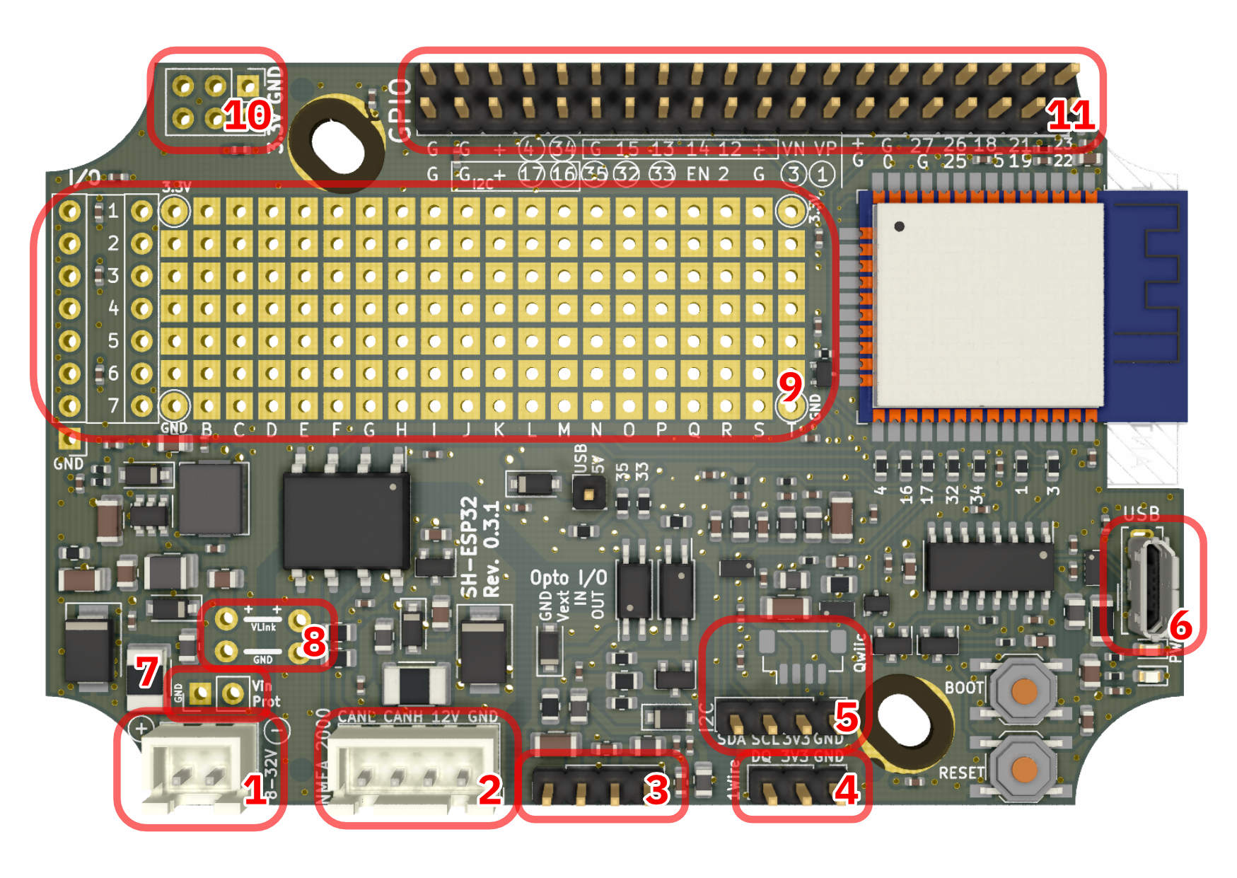
The picture below illustrates the different connectors on the SH-ESP32. The connectors are as follows:
Power connector: A JST XH compatible power connector. A 2.5 mm terminal block can be fitted on the same footprint.
CAN bus connector: A 4-pin JST XH connector designed to be connected to a standard NMEA 2000 compatible DeviceNet M12 connector on the enclosure.
Optocoupler I/O header: Optocoupler input and output can be provided via this interface. The labels for these four pins are a bit “north” on the board: GND, Vext, IN, and OUT.
1-Wire header: 1-Wire interface fitted with ESD protection and noise filtering as well as low-pass filtering required for longer networks. No other circuitry is required for connecting 1-Wire devices to the SH-ESP32. The 1-Wire data in pin (labeled “DQ” on the board is connected to GPIO 4, so in your program, use GPIO 4 as your 1-Wire input pin.)
I2C header: Four-pin header for connecting I2C slave devices to the SH-ESP32. A female header accepts many popular inexpensive OLED display modules using the SSD1306 driver as is.
There is also an unpopulated Qwiic-compatible JST SH footprint next to the 2.54 mm header.
USB: This is your standard USB Micro B connector.
Protected Voltage: These header pads can be used to provide input voltage that has been reverse polarity and surge protected. For example, if you’re powering the board with ~12V, the + pin of these pads will provide ~12V. Observe the polarity: it is opposite of the nearby power input connector.
Voltage link: If you intend to power the board using the NMEA 2000 interface and don’t need galvanic connections to external systems, you can connect these pads together to route the power from the CAN bus connector to the main power supply.
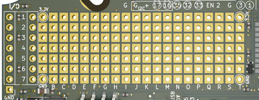
Proto board area: This area can be used for your custom modifications.
Additional voltage output: Use these pads to get additional GND and 3.3V voltage output for any modifications you need. Note that despite what the silkscreen might suggest, the top three pins are all GND and the bottom three are all 3.3V.
GPIO header: The GPIO header provides connections to all GPIO pins available on the ESP32 module. Some of the pins are used by other peripherals by default and need to be enabled using the solder jumpers.
ESP32 module
ESP32 is a series of low-cost, low-power microcontrollers and microcontroller modules created and developed by Espressif Systems, a Shanghai-based Chinese company. The ESP32-WROOM-32 module is built around a powerful dual-core Tensilica Xtensa LX6 microprocessor and features integrated WiFi, dual-mode Bluetooth, and a remarkable amount of peripherals.
The SH-ESP32 features an ESP32-WROOM-32E module with an integrated PCB antenna, while the SH-ESP32-ufl uses ESP32-WROOM-32U that has an U.FL connector for an external antenna.
For more information, visit the ESP32 Wikipedia article, Espressif’s product pages, or read the module datasheet.
Power supply
SH-ESP32 is designed to be used on a boat as easily as possible and includes an 8-32 V switching mode power supply with a maximum efficiency of nearly 90%. The power supply has a 3.3 V output with sufficient output current capability for powering both the ESP32 peak power consumption and any reasonable add-ons.
The power supply includes a self-resetting 500 mA polyfuse, reverse polarity protection, and a hefty TVS protection diode that has a breakdown voltage of 36.7-40.6V and maximum peak pulse dissipation capacity in excess of 600W. Additionally, the power supply includes EMC filtering, designed to keep the conducted emissions of the switching-mode power supply below the regulatory limits.
The switcher IC is Silergy SY8401 that has a wide input range of 4.5-60 V and a maximum output current of 0.8 A.
Peripherals
Buttons and LEDs
There are two buttons and two LEDs on the SH-ESP32. The two buttons are labeled Reset and Boot. The Reset button resets the board by pulling the ESP32 Enable pin low. The Boot button is connected to GPIO0 and can be used during device startup to force the module into a download mode. Otherwise it can be used as a regular button input.
The two LEDs are not explicitly labeled. The red LED is lit whenever there is 3.3V power on the board. The blue LED is connected to GPIO2 (the pin commonly used for LED on ESP32 development boards). It can be controlled by user programs to indicate the state of the device.
USB
The USB interface can be used to reprogram the ESP32 module and to communicate with the user application. It also powers the board when plugged in. The board can be safely powered using the main power connector and USB simultaneously – rectifying diodes ensure that only the highest voltage supply is used.
The USB interface is implemented using a low-cost CH340C USB to serial interface chip. It emulates a standard serial interface with bit rates of up to 2 Mbps.
CH340 chips are natively supported by Linux kernels but require a driver on Mac and Windows. The driver can be downloaded from the manufacturer website.
CAN bus (NMEA 2000)
NMEA 2000 is a ubiquitous communications standard used for connecting sensor, control, and display devices on boats and ships. It is based on the Controller Area Network (CAN bus) which is a vehicle bus standard designed to allow devices to communicate with each other without a host computer.
SH-ESP32 includes an isolated CAN bus interface that allows safe and NMEA 2000 compliant interconnection of devices. The CAN bus interface can be used to directly output sensor readings to the NMEA 2000 network, or to build NMEA 2000 gateways or similar devices.
The CAN interface uses ESP32’s integrated CAN controller and the ISO1050DUB isolated CAN transceiver by Texas Instruments. It features support for high isolation voltages and transients, and bit rates of up to 1 Mbps.
The CAN bus interface can also be used to power the whole device if there are no galvanic connections to other external systems. (FIXME: Needs a more thorough description and illustration.)
The CAN interface includes a built-in termination resistor that can be enabled by closing the “CAN term” solder jumper on the bottom side of the board.
I2C
I2C (Inter-Integrated Circuit) is a very popular synchronous serial communication bus commonly used for interfacing with a number of different ICs. It uses two data wires in addition to voltage and ground.
I2C can be used to connect a large number of devices to the SH-ESP32. Device types include analog-to-digital converters, attitude sensors, temperature and humidity sensors, displays, keypads, GPS, and so on. Any Qwiic-compatible board from SparkFun can be used with the SH-ESP32 by splicing the wires or by adding a JST SH compatible connector to the available footprint.
Maximum I2C bus distances depend on the load, but should be less than 3-4 m. There are better suited protocols for long distance communication.
1-Wire
1-Wire is a device communications bus system designed by Dallas Semiconductor, since acquired by Maxim Integrated Products. Although 1-Wire is a slow-speed protocol, supporting only speeds up to 16.3 kbps, it is very simple to implement and can be used over long distances. It is commonly used for temperature sensors and similar simple sensing devices.
The SH-ESP32 1-Wire implementation features ESD and RF noise filtering as well as low-pass filtering to improve network reliability.
Note that the 1-Wire data pin (labeled “DQ”) is physically mapped to GPIO4, so in your program, use GPIO4 for all 1-Wire data.
Optocoupler input and output
Optocoupler input and output is the recommended way to add simple digital signal input and output and sensing to different external systems. It can be used e.g. to count alternator pulses for RPM measurement or switch relays on or off.
Additionally, the SH-ESP32 opto I/O implementation should be able to drive slow-speed single-side NMEA 0183 interfaces.
The absolute maximum voltage for the optocoupler input is 18V but it can be extended by adding an additional current-limiting resistor in series to the input.
If you provide a voltage between about 2.5V and 18V in ISO IN, you’ll have the output of the input optocoupler pulled high, meaning that OPTO_IN (GPIO 35) is pulled high.
Likewise, if you pull OPTO_OUT (GPIO 33) high, that will make the ISO_OUT pin be driven to the voltage you have supplied to the Vext pin.
It is possible to drive small automotive relays using the optocoupler output. In that case, the solenoid pins should be connected to the Vext and OUT pins.
GPIO header
The GPIO header can be used to access all GPIO pins of the ESP32 module. The silkscreen labeling next to the header refers to the GPIO numbers of the pins.

Circled numbers are by default used by other peripherals and have to be connected by setting the solder jumpers (see Section “Customizing GPIO assignments” for more information).
The pin group including GPIOs 16 and 17 encapsulated by a rectangle can be used as duplicate I2C header if the respective solder jumpers are closed.
The pin group with GPIOs 12-15 can be used as a JTAG connector with some simple external hardware and software. JTAG is an industry-standard debugging interface for microcontrollers and other programmable devices that allows on-chip debugging, including setting hardware breakpoints, stepping through code and inspecting live variable values.
Finally, the pin group consisting of the 14 pins on the right end of the header will be used by an Ethernet add-on board.
No ESD, RF noise protection or other filtering is provided for the GPIO header pins.
Proto board area
The large open area in the middle of the SH-ESP32 is the proto board area. It can be used to add new functionality via embedded 3rd party modules or THT circuitry. Layer fills or traces on the inner copper layers are on purpose avoiding the proto board area, and the area can be safely drilled or modified to accept larger components, if needed. There are traces very close to the area, however, so some care should be taken when modifying the pads at the border of the area.
The round pads to the left hand side that are labeled 1 - 7 are horizontally connected. That is, the round pad on the left side of the label “1” is connected to the round pad on the right side of the label “1”, and so on for 2 - 7. This is to make it easier to place a header on the PCB edge. You can place a header on the row at the edge and make connections to the inner row of round pads.
Pinouts of peripherals
The ESP32 has a GPIO matrix that allows most of the digital GPIO functionality to be mapped freely to any GPIO. This is utilized extensively on SH-ESP32, and few peripherals are mapped to their standard pins. The GPIO pinout of different peripherals is given below. Unlisted pins are not used by SH-ESP32 and can be utilized freely.
The GPIOs having a mark in the Jumper column are, by default, connected to the respective peripheral and disconnected from the GPIO header. These connections may be altered by modifying the jumpers as described in Section “Customizing GPIO assignments”. For example, GPIO4 is circled on the board, and in the table below, there is an “X” in the Jumper column, and “1-Wire data” in the Function column. This means that, unless you do some soldering, the pin that’s labeled 4 isn’t connected to anything, because the 1-Wire data pin (“DQ”) is connected to GPIO4 by default.
The ADC column lists pins connected to either of the ESP32’s two ADCs. ADC2 is used by the WiFi, so if WiFi is in use, ADC2 cannot be used.
Touch N refer to the capacitive touch sensor inputs.
| GPIO # | Jumper | ADC | Function | Optional Function |
|---|---|---|---|---|
| 00 | 2 | BOOT | Ethernet REF_CLK; Touch 1 | |
| 01 | x | Serial TXD0 | ||
| 02 | 2 | Blue LED | Touch 2 | |
| 03 | x | Serial RXD0 | ||
| 04 | x | 2 | 1-Wire data | Touch 0 |
| 05 | Free | Ethernet Reset_N | ||
| 12 | 2 | Free | JTAG TDI; Touch 5 | |
| 13 | Free | JTAG TCK; Touch 4 | ||
| 14 | 2 | Free | JTAG TMS; Touch 6 | |
| 15 | 2 | Free | JTAG TDO; Touch 3 | |
| 16 | x | I2C SDA | ||
| 17 | x | I2C SCL | ||
| 18 | Free | Ethernet MDIO | ||
| 19 | Free | Ethernet TXD[0] | ||
| 21 | Free | Ethernet TX_EN | ||
| 22 | Free | Ethernet TXD[1] | ||
| 23 | Free | Ethernet MDC | ||
| 25 | 2 | Free | Ethernet RXD[0] | |
| 26 | 2 | Free | Ethernet RXD[1] | |
| 27 | 2 | Free | Ethernet CRS_DV; Touch 7 | |
| 32 | x | 1 | CAN TX | Touch 9 |
| 33 | x | 1 | Opto OUT | Touch 8 |
| 34 | x | 1 | CAN RX, input only | |
| 35 | x | 1 | Opto IN, input only | |
| 36 (VP) | 1 | Free, input only | ||
| 39 (VN) | 1 | Free, input only |
This page provides a great description of the different ESP32 GPIOs and their availability.
Customizing GPIO assignments
Nearly all hard-wired peripherals can be disconnected by unsoldering a 0R resistor jumper on the board top layer. In a similar fashion, the solder jumpers on the bottom layer can be closed to connect the GPIO pin to the respective GPIO header pin. The resistor and solder jumpers are illustrated in figures below.
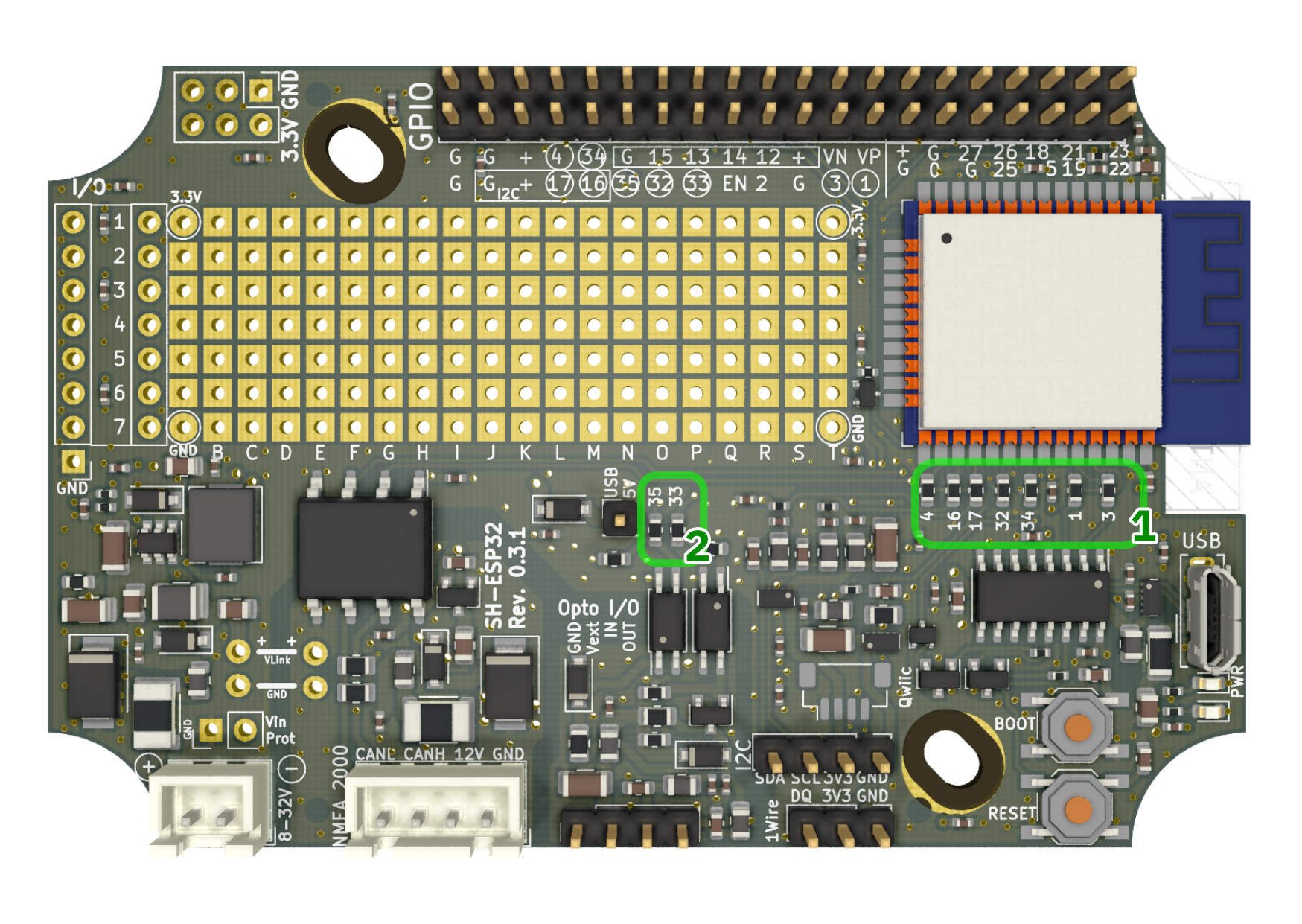 Resistor jumpers on the top layer. To disconnect the GPIO pin from any peripheral, unsolder the respective jumper.
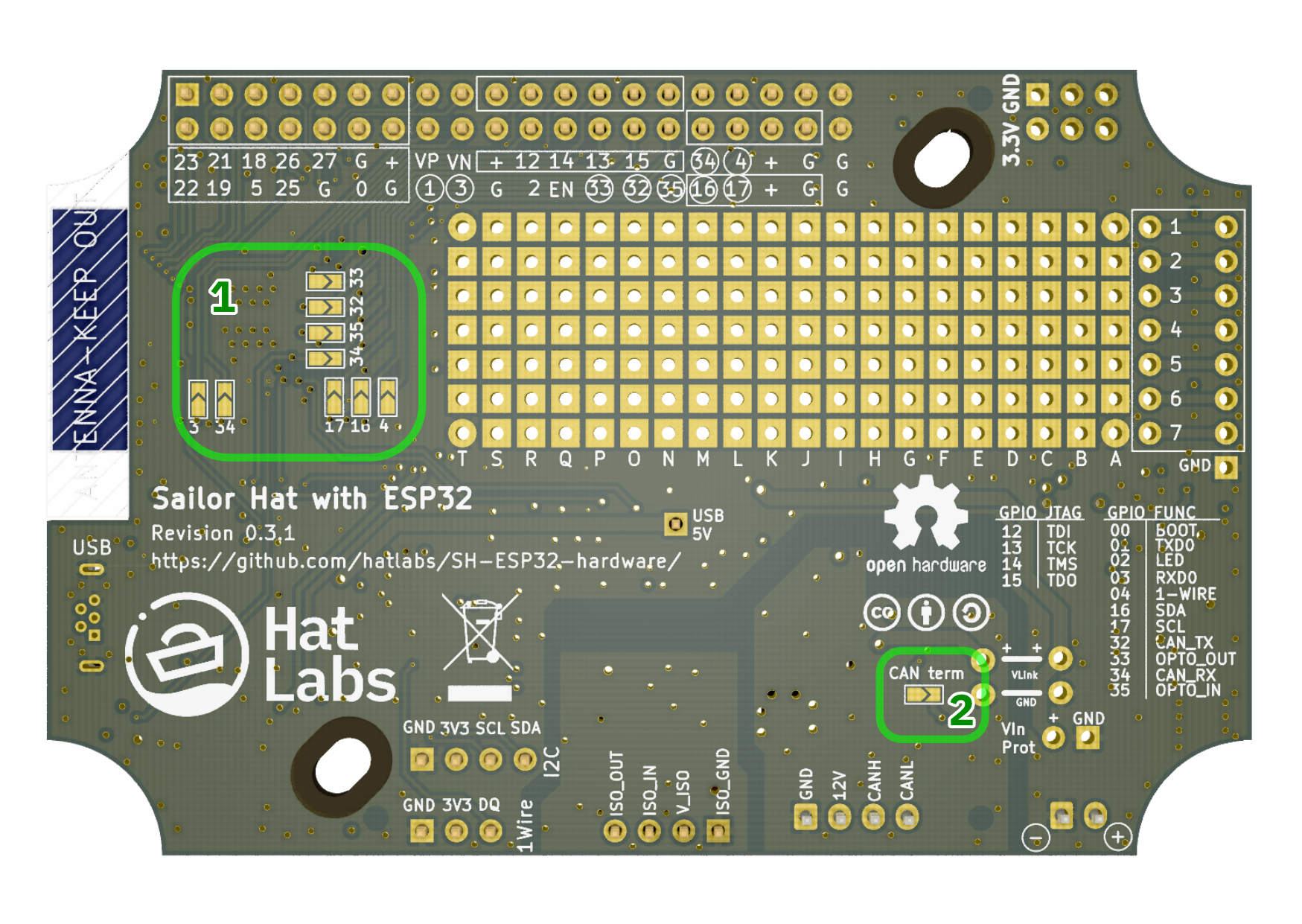 Solder jumpers on the bottom layer. To connect a GPIO pin to the GPIO header, close the solder jumper by adding a blob of solder on top of the jumper area.
For example, if don’t need the CAN interface and want to reuse the GPIOs 32 and 34 on the GPIO header, desolder the resistors labeled 32 and 34 next to the ESP32 module to disconnect the module from the CAN interface. Then close the solder jumpers labeled 32 and 34 to connect the GPIO pins to the GPIO header.
Likewise, if you want to enable I2C both on the GPIO header and the dedicated I2C connector, close the solder jumpers 16 and 17 on the board bottom layer.
Finally, the jumpers on either side can be used to customize the GPIO assignments. For example, if you want to swap 1-Wire data pin from GPIO4 to GPIO15, you can unsolder the GPIO4 resistor jumper and add a jumper wire from either the ESP32 module pad or the GPIO header to the lower resistor jumper pad.
Note: The silkscreen labeling for GPIO 1 and 3 solder jumpers is incorrect in revision 0.3.1 devices. They are labeled 3 and 34 while the correct labeling is 1 and 3.
